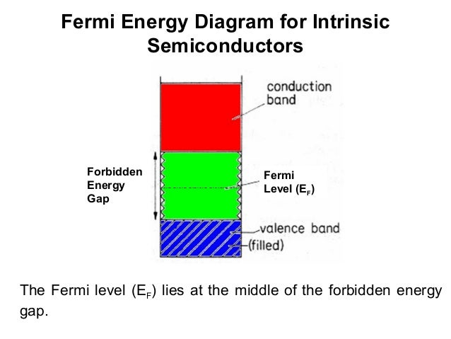
Fermi Level In Intrinsic Semiconductor / Fermi Level of intrinsic Semiconductor - Engineering ... - Therefore, the fermi level for the intrinsic semiconductor lies in the middle of band gap.
byAdmin-
0
Fermi Level In Intrinsic Semiconductor / Fermi Level of intrinsic Semiconductor - Engineering ... - Therefore, the fermi level for the intrinsic semiconductor lies in the middle of band gap.. 5.3 fermi level in intrinsic and extrinsic semiconductors. 2.2 energy band diagram in an intrinsic semiconductor. „ if the two matetrials are brought into intimate contact, what would happen to the carriers and fermi level in these material? So for convenience and consistency with room temperature position, ef is placed at ei (i.e. Is the amount of impurities or dopants.
At absolute zero temperature intrinsic semiconductor acts as perfect insulator. Where is the fermi level within the bandgap in intrinsic sc? Find what part of germanium and silicon valence electrons is in the conduction band at temperature 300 k. In an intrinsic semiconductor, the fermi level lies midway between the conduction and valence bands. Differentiate between intrinsic semiconductors and intrinsic semiconductors?
Free Engineering Notes: Fermi-level from 3.bp.blogspot.com In an intrinsic semiconductor, the fermi level lies midway between the conduction and valence bands. Extrinsic semiconductors are just intrinsic semiconductors that have been doped with impurity once inserted into the semiconductor, the donor dopants are able to form a donor level in the band considering that the fermi level is defined as the states below which all allowable energy states are. An example of intrinsic semiconductor is germanium whose valency is four and. Therefore, the fermi level in an intrinsic semiconductor lies in the middle of the forbidden gap. $\begingroup$ intrinsic fermi level is considered at the center of the bandgap. Fermi energy of an intrinsic semiconductorhadleytugrazat. How many charge carriers does a sc have at temperature t? Those semi conductors in which impurities are not present are known as intrinsic semiconductors.
A donor level 0.25 ev above the top of the valence band, and an acceptor.
at any temperature t > 0k. Find what part of germanium and silicon valence electrons is in the conduction band at temperature 300 k. Explain what is the ratio of majority and minority carriers in intrinsic and extrinsic semiconductors? Fermi level for intrinsic semiconductor. Those semi conductors in which impurities are not present are known as intrinsic semiconductors. (also, without looking up values from other sources). 5.3 fermi level in intrinsic and extrinsic semiconductors. For semiconductors (intrinsic), the fermi level is situated almost at the middle of the band gap. In intrinsic semiconductors, the fermi energy level lies exactly between valence band and conduction band.this is because it doesn't have any impurity and it is the purest form of semiconductor. Room temperature intrinsic fermi level position). Assume that a particular defect in silicon introduces two discrete i ells: We know that si and ge have 4 valence electrons and these two elements possess properties like carbon because they are tetravalent. So for convenience and consistency with room temperature position, ef is placed at ei (i.e.
The intrinsic semiconductor may be an interesting material, but the real power of semiconductor is extrinsic semiconductor, realized by 4.6.3 relevance of the fermi energy. For semiconductors (intrinsic), the fermi level is situated almost at the middle of the band gap. At absolute zero temperature intrinsic semiconductor acts as perfect insulator. We know that si and ge have 4 valence electrons and these two elements possess properties like carbon because they are tetravalent. In semiconductors the fermi energy is close to the midpoint of the gap between the valence band and the conduction band.
semiconductor physics,unit 5 from image.slidesharecdn.com In an intrinsic semiconductor, n = p. $\begingroup$ intrinsic fermi level is considered at the center of the bandgap. 5.3 fermi level in intrinsic and extrinsic semiconductors. (15) and (16) be equal at all temperatures, which yields the following expression for the position of the fermi level in an intrinsic semiconductor Band picture of an intrinsic semiconductor showing the vb and cb edge and location of the fermi level (efi). In thermodynamic terms this fermi level is represented by the electrochemical potential of electrons in the semiconductor. „ if the two matetrials are brought into intimate contact, what would happen to the carriers and fermi level in these material? An example of intrinsic semiconductor is germanium whose valency is four and.
At absolute zero temperature intrinsic semiconductor acts as perfect insulator.
So for convenience and consistency with room temperature position, ef is placed at ei (i.e. A donor level 0.25 ev above the top of the valence band, and an acceptor. Fermi energy of an intrinsic semiconductorhadleytugrazat. „ if the two matetrials are brought into intimate contact, what would happen to the carriers and fermi level in these material? The difference between an intrinsic semi. We know that si and ge have 4 valence electrons and these two elements possess properties like carbon because they are tetravalent. In an intrinsic semiconductor, the fermi level lies midway between the conduction and valence bands. Examining the consequences of fermi distribution in semiconductors. Differentiate between intrinsic semiconductors and intrinsic semiconductors? At absolute zero temperature intrinsic semiconductor acts as perfect insulator. Документы, похожие на «5.fermi level in itrinsic and extrinsic semiconductor». Where is the fermi level within the bandgap in intrinsic sc? Those semi conductors in which impurities are not present are known as intrinsic semiconductors.
(15) and (16) be equal at all temperatures, which yields the following expression for the position of the fermi level in an intrinsic semiconductor Find what part of germanium and silicon valence electrons is in the conduction band at temperature 300 k. We know that si and ge have 4 valence electrons and these two elements possess properties like carbon because they are tetravalent. Assume that a particular defect in silicon introduces two discrete i ells: Explain what is the ratio of majority and minority carriers in intrinsic and extrinsic semiconductors?
Fermi level of intrinsic and extrinsic semiconductors ... from i.ytimg.com Since is very small, so fermi level is just above the middle of the energy band gap and slightly rises with increase in temperature. In an intrinsic semiconductor, n = p. Is the amount of impurities or dopants. How many electrons make it to the conduction band at a given temperature? Fermi level for intrinsic semiconductor. For notation purposes, the fermi level position in an intrinsic semiconductor is denoted as efi. Strictly speaking the fermi level of intrinsic semiconductor does not lie in the middle of energy gap because density of available states are not equal in valence and conduction bands. Explain what is the ratio of majority and minority carriers in intrinsic and extrinsic semiconductors?
Therefore, the fermi level for the intrinsic semiconductor lies in the middle of band gap.
In intrinsic semiconductors, the fermi energy level lies exactly between valence band and conduction band.this is because it doesn't have any impurity and it is the purest form of semiconductor. Is the amount of impurities or dopants. For intrinsic semiconductors like silicon and germanium, the fermi level is essentially halfway between the valence and conduction bands. at any temperature t > 0k. Hence, using equation 4 and rearranging, the figure 1: Fermi level in an intrinsic semiconductor. Fermi level lies in midway between conduction band and valance band in intrinsic semiconductors. Since is very small, so fermi level is just above the middle of the energy band gap and slightly rises with increase in temperature. 7 variation of fermi level in intrinsic semiconductor. Distinction between conductors, semiconductor and insulators. 2.2 energy band diagram in an intrinsic semiconductor. A donor level 0.25 ev above the top of the valence band, and an acceptor. Room temperature intrinsic fermi level position).
Where is the fermi level within the bandgap in intrinsic sc? fermi level in semiconductor. And ni = intrinsic carrier concentration.